What is CPLD (Complex Programmable Logic Device)?

Programmable Logic II: Program a CPLD from start to finish.
Catalog |
Ⅰ Device Introduction
CPLD (Complex Programmable Logic Device) is mainly composed of programmable logic macrocells (MC) around the center of the programmable interconnect matrix cell. Among them, the MC structure is more complex and has a complex I/O cell interconnection structure, which can be generated by the user according to the needs of a specific circuit structure to complete certain functions. Since the CPLD uses fixed-length metal wires for the interconnection of each logic block internally, the designed logic circuits are time-predictable, avoiding the disadvantage that the timing of segmented interconnection structure is not completely predictable.
Development History
In the 1970s, the earliest programmable logic device, the PLD, was born. Its output structure was programmable logic macrocells. Because its hardware structure design could be done by software, its design was highly flexible compared to that of pure hardware digital circuits. But its overly simple structure also made them capable of implementing only small-scale circuits. To make up for this shortcoming that PLDs can only design small-scale circuits, complex programmable logic devices - CPLDs - were introduced in the mid-1980s.
Device Features
CPLD has the features of flexible programming, high integration, short design and development cycle, wide applicability, advanced development tools, low design and manufacturing cost, low hardware experience requirement for designers, no testing required for standard products, high confidentiality, and affordable pricing. It can realize larger scale circuit design, so it is widely used in product prototyping and product production (generally below 10,000 pieces). CPLD devices have become an indispensable part of electronic products, and their design and application have become a necessary skill for electronic engineers.
How to use CPLDs?
CPLD is a kind of digital integrated circuit that users construct their own logic functions according to their needs. The basic design method is to use the integrated development software platform to generate the corresponding target file by using schematic diagram and hardware description language and then transfer the code to the target chip through the download cable ("in-system" programming) to realize the designed digital system.
Here is the design process of the responder system as an example, i.e. the design flow of the chip. Most of the work of the CPLD is done on the computer. Open the integrated development software (such as Intel Quartus for Altera/Intel devices, or Vivado/ISE for AMD Xilinx devices) → draw a schematic diagram, write hardware description language (VHDL, Verilog) → compile → give the input excitation signal of the logic circuit, simulate, and check whether the logic output result is correct → carry out pin input and output locking (e.g., 64 input and output pins of EPM7128 can be set as needed) → generate code → transfer and store the code in the CPLD chip through the download cable.
The chip pins interface with components such as digital displays, quiz switches, indicators, and buzzers through wires to the board.
The system interface circuit using CPLD chip is then powered on for testing. When the quiz switch is pressed, the indicator light of the corresponding bit should be on. After the answer is correct, the referee will add points to see if the digital display is correct at this time. If you find any problem, you can modify the schematic diagram or hardware description language again to improve the design. After the design, such as mass production, you can directly copy other CPLD chips, that is, write the code. If you want to do other designs on the chip, such as traffic light design, you have to draw the schematic diagram or write the hardware description language again, and repeat the above work process to complete the design. This modification of the design is equivalent to redecorating the house, and this reprogramming can be performed tens of thousands of times for CPLDs.

System interface circuit using CPLD chip
Family members
After decades of development, many companies have developed CPLD programmable logic devices. The more typical ones are the products of Intel (formerly Altera), Lattice, and AMD (formerly Xilinx), three major companies in the programmable logic industry. Some commonly used chips include:
Intel (Altera) EPM7128S (PLCC84) - Note: Intel acquired Altera in 2015 and spun it out as an independent company again in 2025
Lattice LC4128V (TQFP100)
AMD Xilinx XC95108 (PLCC84) - Note: AMD acquired Xilinx in 2022. However, many older CPLD product lines including XC9500XL and CoolRunner series have been discontinued as of 2024
Important Update (2024-2025): The CPLD market has seen significant changes. AMD (Xilinx) announced discontinuation of several legacy CPLD product lines including XC9500XL, CoolRunner XPLA3, and CoolRunner II series in 2024. Designers should consult current product availability before selecting CPLDs for new designs.
Ⅱ Composition of CPLD
A CPLD consists of three main components: a logic block, a programmable interconnect channel, and an I/O block.
The logic block in CPLD is similar to a small-scale PLD. Usually, a logic block contains 4 to 20 macrocells, each of which is generally composed of a product term array, product term assignment, and programmable registers. Each macrocell has multiple configurations, and each macrocell can be used in cascade, so that more complex combinational logic and timing logic functions can be realized. For highly integrated CPLDs, embedded array blocks with on-chip RAM/ROM are usually provided.
Programmable interconnect channels provide interconnection networks between logic blocks, macrocells, and input/output pins. The input/output blocks (I/O blocks) provide the interface between the internal logic and the I/O pins of the device.

The composition of CPLD
CPLDs with larger logic scales generally also have built-in JTAG boundary-scan test circuitry, which allows for comprehensive and thorough system testing of programmed high-density programmable logic devices, in addition to in-system programming via the JTAG interface.
Due to the different integration processes, integration scale, and manufacturers, there are also major differences in the partition structure and logic cells of various CPLDs.
Ⅲ Structure of CPLD
EPM7128S device
(1) EPM7128S device basic structure
EPM7128S device mainly consists of logic array block LAB, macrocells, I/O control block and programmable interconnect array PIA.
In the multi-array matrix structure, each macrocell has a programmable AND array and a fixed OR array, as well as a configurable flip-flop with independently programmable clock, clock enable, clear, and reset functions. Multiple LABs are connected via the Programmable Interconnect Array PIA and the global bus. Each LAB is also connected to the corresponding I/O control module to provide direct input and output channels.
(2) EPM7128S Macrocell Structure
Each macrocell of the EPM7128S is capable of being individually configured for combinational or timing logic operation. The macrocell consists of three main parts: the logic array, the product term selection matrix, and the programmable registers. The programmable registers can be programmed to bypass and implement combinational logic according to the logic needs. If used as registers, the corresponding programmable logic device development software will select the effective register operation according to the design logic needs to minimize the device resources used for the design.
XCR3064XL Device
The XCR3064XL device macrocell structure consists of function blocks and I/O cells connected by zero power interconnect arrays, with each logic block containing 16 macrocells.
Ⅳ Identification and Classification of FPGAs and CPLDs
The identification and classification of FPGAs and CPLDs are mainly based on their structural characteristics and operating principles.
The usual classification methods are:
Devices that are structured in a product term manner to form logical behavior are called CPLDs, such as Lattice's ispLSI series, AMD Xilinx's XC9500 series (now discontinued), Intel Altera's MAX7000S series, and Lattice's (formerly Vantis) Mach series.
Devices that are structured using a look-up table method to form the logic behavior are called FPGAs, such as AMD Xilinx's Spartan series, Intel Altera's FLEX10K or ACEX1K series, etc.
Although FPGA and CPLD are both programmable ASIC devices and have many common features, they have their own characteristics due to the differences in the structure of CPLD and FPGA:
① CPLD is more suitable for completing various algorithms and combinational logic, and FPGA is more suitable for completing timing logic. In other words, FPGA is more suitable for structures with rich flip-flops, while CPLD is more suitable for structures with limited flip-flops and rich product terms.
② The continuous wiring structure of CPLD determines that its timing delays are uniform and predictable, while the segmented wiring structure of FPGA determines the unpredictability of its delays.
③ CPLD is programmed by modifying the logic function with fixed interconnect circuit, while FPGA is programmed by changing the routing of internal wires; FPGA can be programmed at the logic gate level, while CPLD is programmed at the logic block level.
④ FPGAs are more integrated than CPLDs and have more complex wiring structures and logic implementations.
⑤ CPLD is more convenient to use than FPGA. CPLD is programmed by EEPROM or FLASH technology, no external memory chip is needed, making it easy to use. While the FPGA programming information needs to be stored in external memory, the use is more complex.
⑥ CPLDs are faster than FPGAs and have greater time predictability. This is due to the fact that FPGAs are programmed at the gate level and use distributed interconnections between CLBs, while CPLDs are programmed at the logic block level and their interconnections between logic blocks are collective.
⑦ CPLD is mainly based on EEPROM or FLASH memory programming, which can be programmed up to 10,000 times, and has the advantage that the programming information is not lost even when the system is powered off.
CPLD can be further divided into two categories: programming on the programmer and programming in the system. FPGA is mostly based on SRAM programming, and the programming information is lost when the system is powered off, and the programming data needs to be rewritten into SRAM from outside the device each time it is powered up. The advantage is that it can be programmed any number of times and can be programmed quickly in operation, thus achieving dynamic configuration at the board level and system level.
⑧ CPLD confidentiality is good, FPGA confidentiality is relatively poor.
⑨ In general, the power consumption of CPLD is greater than that of FPGA, and the higher the integration level, the more obvious the difference becomes.
Article Updated: October 2025 - Corrections made to reflect current industry status including company acquisitions (Intel/Altera, AMD/Xilinx), product discontinuations, and corrected technical terminology and spelling errors.
1. What is CPLD used for?
CPLD is used for loading the configuration data of a field programmable gate array from non-volatile memory. CPLDs are frequently used many applications like in cost sensitive, battery operated portable devices due to its low size and usage of low power.
2. What is CPLD in digital logic?
A programmable logic device (PLD) is an electronic component used to build reconfigurable digital circuits. Unlike integrated circuits (IC) which consist of logic gates and have a fixed function, a PLD has an undefined function at the time of manufacture.
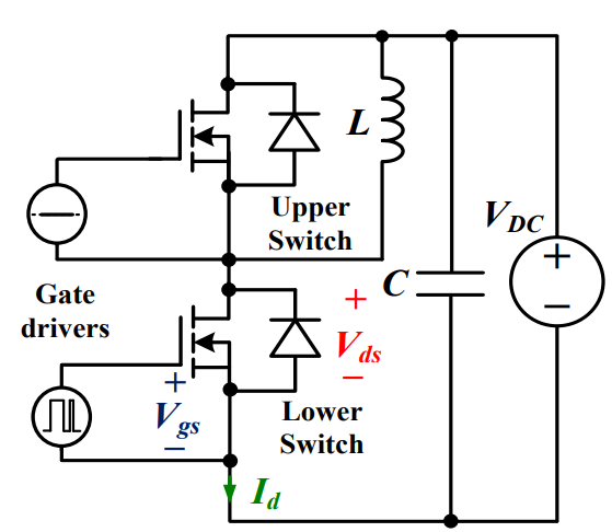 Discovering New and Advanced Methodology for Determining the Dynamic Characterization of Wide Bandgap DevicesSaumitra Jagdale15 March 20242501
For a long era, silicon has stood out as the primary material for fabricating electronic devices due to its affordability, moderate efficiency, and performance capabilities. Despite its widespread use, silicon faces several limitations that render it unsuitable for applications involving high power and elevated temperatures. As technological advancements continue and the industry demands enhanced efficiency from devices, these limitations become increasingly vivid. In the quest for electronic devices that are more potent, efficient, and compact, wide bandgap materials are emerging as a dominant player. Their superiority over silicon in crucial aspects such as efficiency, higher junction temperatures, power density, thinner drift regions, and faster switching speeds positions them as the preferred materials for the future of power electronics.
Read More A Comprehensive Guide to FPGA Development BoardsUTMEL11 September 202515709
This comprehensive guide will take you on a journey through the fascinating world of FPGA development boards. We’ll explore what they are, how they differ from microcontrollers, and most importantly, how to choose the perfect board for your needs. Whether you’re a seasoned engineer or a curious hobbyist, prepare to unlock new possibilities in hardware design and accelerate your projects. We’ll cover everything from budget-friendly options to specialized boards for image processing, delve into popular learning paths, and even provide insights into essential software like Vivado. By the end of this article, you’ll have a clear roadmap to navigate the FPGA landscape and make informed decisions for your next groundbreaking endeavor.
Read More Applications of FPGAs in Artificial Intelligence: A Comprehensive GuideUTMEL29 August 20253849
This comprehensive guide explores FPGAs as powerful AI accelerators that offer distinct advantages over traditional GPUs and CPUs. FPGAs provide reconfigurable hardware that can be customized for specific AI workloads, delivering superior energy efficiency, ultra-low latency, and deterministic performance—particularly valuable for edge AI applications. While GPUs excel at parallel processing for training, FPGAs shine in inference tasks through their adaptability and power optimization. The document covers practical implementation challenges, including development complexity and resource constraints, while highlighting solutions like High-Level Synthesis tools and vendor-specific AI development suites from Intel and AMD/Xilinx. Real-world applications span telecommunications, healthcare, autonomous vehicles, and financial services, demonstrating FPGAs' versatility in mission-critical systems requiring real-time processing and minimal power consumption.
Read More 800G Optical Transceivers: The Guide for AI Data CentersUTMEL24 December 20254576
The complete guide to 800G Optical Transceiver standards (QSFP-DD vs. OSFP). Overcome supply shortages and scale your AI data center with Utmel Electronic.
Read More The 2026 Engineer’s Guide: Choosing the Right MCU for Your Next IoT & New Energy ProjectUTMEL30 April 202635
A comprehensive comparison of 2026's leading MCUs from ST, NXP, and Microchip across power efficiency, processing performance, connectivity, and ecosystems to help engineers select the optimal chip for next-gen IoT and new energy projects.
Read More
Subscribe to Utmel !
![80HCPS1432CRM]() 80HCPS1432CRM
80HCPS1432CRMRenesas Electronics America Inc.
![SI8261BBD-C-IS]() SI8261BBD-C-IS
SI8261BBD-C-ISSilicon Labs
![SI8261BAD-C-IS]() SI8261BAD-C-IS
SI8261BAD-C-ISSilicon Labs
![FOD8333]() FOD8333
FOD8333ON Semiconductor
![FOD8332R2]() FOD8332R2
FOD8332R2ON Semiconductor
![ACPL-302J-500E]() ACPL-302J-500E
ACPL-302J-500EBroadcom Limited
![SI8275GB-IS1]() SI8275GB-IS1
SI8275GB-IS1Silicon Labs
![SI8238AD-D-IS3]() SI8238AD-D-IS3
SI8238AD-D-IS3Silicon Labs
![FOD3120SD]() FOD3120SD
FOD3120SDON Semiconductor
![ADUM3223BRZ]() ADUM3223BRZ
ADUM3223BRZAnalog Devices Inc.


 Product
 Brand
Brand Articles
 Tools
Tools


